Nanostructured superconducting materials
V. Yu. Lyakhno, S. V. Bengus, O. O. Leha, O. V. Zraichenko, M. Yu. Mikhailov
We study artificial layered and granular low dimensional superconducting systems
Phenomena:
- single photon absorbtion in SC nanowires
- intrinsic pinning and vortex lattice in multilayers
- superconductor-insulator transition
Objects:
- thin superconducting films
- metal-insulator multilayers
- heterostructures of A4B6
- sol-gel granular films
Superconducting nanowire single photon detectors (SNSPDs)
SNSPDs are highly efficient single photon detectors of visible and near infrared radiation based on superconducting nanowires patterned out of ultrathin films. The current choice of superconducting materials suitable for SNSPD development is limited. Prior to nanostructuring, the as-deposited ultrathin films should provide a continuous surface down to few nanometers thickness. Of all materials for use as SNSPDs studied so far, the only commercially available SNSPD detectors are made of crystalline NbN, NbTiN and amorphous WSi ultrathin films. Particularly important is the possibility for uniform deposition across large areas in order to achieve uniform templates for later detector manufacture.
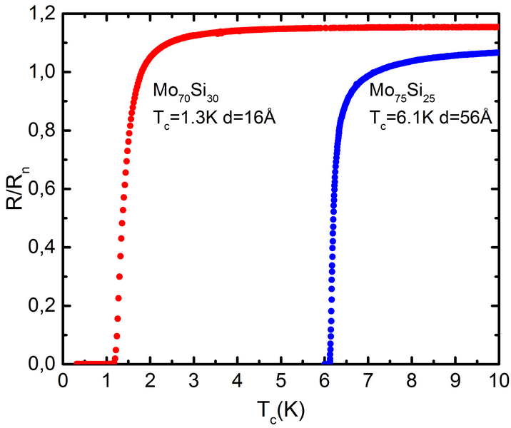
We are involved in the development of new materials for SNSPDs. We have studied superconducting properties of ultrathin amorphous molybdenum silicon and tungsten silicon films. For the first time, we developed an efficient superconducting single photon detector made of amorphous MoSi film. The critical temperature of the studied amorphous films can be easily tuned by thickness or stoichiometry. We deposit our ultrathin amorphous films by magnetron co-sputtering from two targets onto rotating substrate. We were able to demonstrate 18 % of detection efficiency for 1200 nm wavelength at 1.8K, a response time 6 ns and timing jitter of 120 ps for MoSi-based SNSPDs [ ,
,  , arxiv; ,
  ].
].
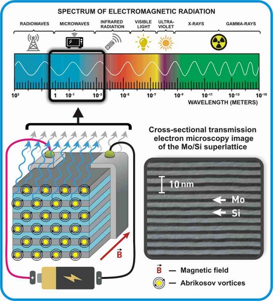
Microwave emission from superconducting vortices in Mo/Si multilayers
Most of superconductors in a magnetic field are penetrated by a lattice of quantized flux vortices. In the presence of a transport current causing the vortices to cross sample edges, emission of electromagnetic waves is expected due to the continuity of tangential components of the fields at the surface. Yet, such a radiation has not been observed so far due to low radiated power levels and lacking coherence in the vortex motion. In our recent paper (Nature Communications), we clearly evidence the emission of electromagnetic waves from vortices crossing the layers of a superconductor/insulator Mo/Si superlattice. The emission spectra consist of narrow harmonically related peaks which can be finely tuned in the GHz range by the dc bias current and, coarsely, by the in-plane magnetic field value. Our findings show that superconductor/insulator superlattices can act as dc-tunable microwave generators bridging the frequency gap between conventional radiofrequency oscillators and (sub-)terahertz generators relying upon the Josephson effect.
M.Yu. Mikhailov, O.I. Yuzephovich.
Superconducting heterostructures AIVBVI
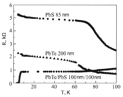
The heterostructures are made of chalcogenides: PbS, PbSe, PbTe, YbS, YbSe, YbTe, EuS, EuSe, EuTe. They are semiconductors with the crystal lattice of NaCl-type. The difference in crystal lattice periods is compensated by the formation of misfit dislocation grid at the interface between layers. The grid's period varies from 5.2 to 23nm depending on the combination of semiconductors.
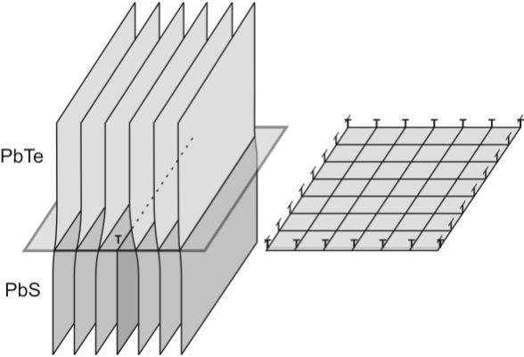

If at least one of the semiconductors is narrow-gap, the elastic stress field along the dislocation lines cause the band inversion in it and free charge carriers appear. The dislocation net acquires metallic properties that results in the metallic-type conductivity at the interface.
At low temperatures the heterostructures exhibit superconductivity with critical temperatures Tc ≤ 6.5K. The superconductivity is inherent only to the heterostructures, while individual films are semiconductors.
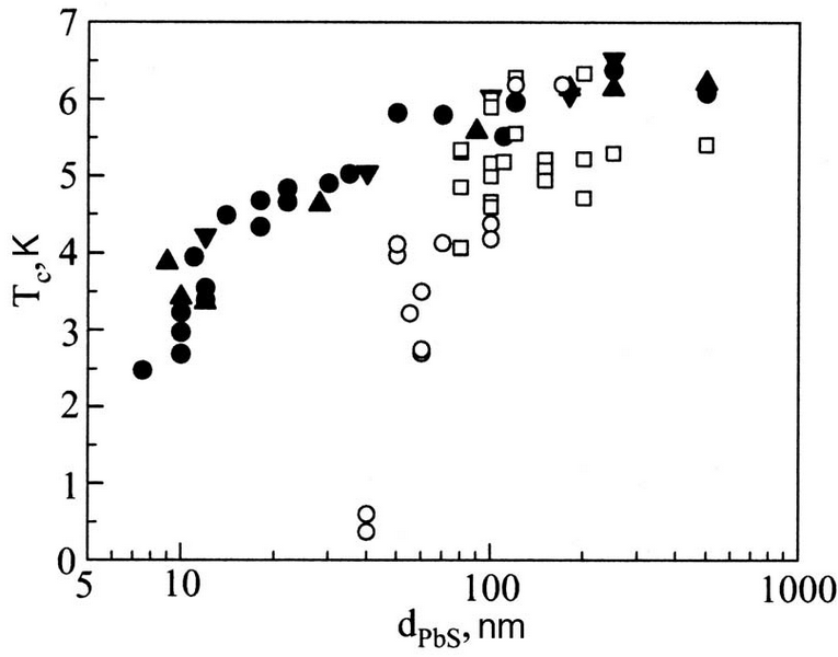
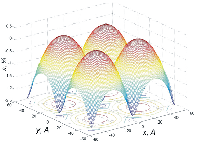
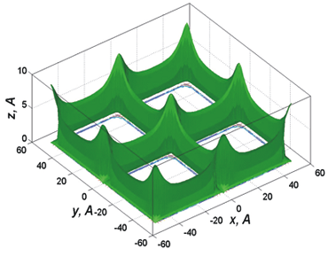
The dimensionality and period of the self-organized superconducting nanostructures in semiconductor heterostructures can be changed by the choice of the type of semiconductors, the thickness of the semiconductor layers, and their number. It is possible to produce:
- arrays of quantum dots with a single Josephson weak links;
- continuous superconducting nanonets;
- quasi-3D structures - multilayers.
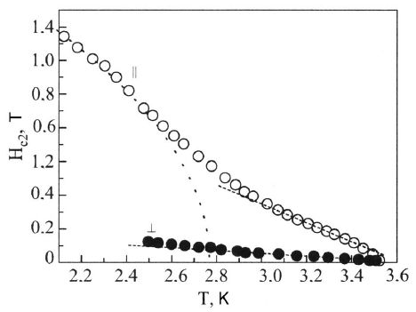
The dimensionality and anisotropy of these heterostructures can be seen from the behaviour of upper critical magnetic fields. The superlattices exhibit 3d-behavior near Tc and at lower temperatures the dimensional crossover to 2d-bevahior is observed.
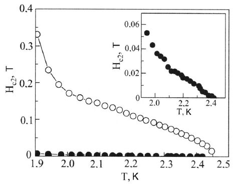
The critical magnetic fields of bilayer sandwiches are more anisotropic. The dimensional crossover from 2d- to 1d-behaviour is observed. A sharp divergence for the perpendicular critical magnetic field dependence is characteristic of superconducting nanonets.
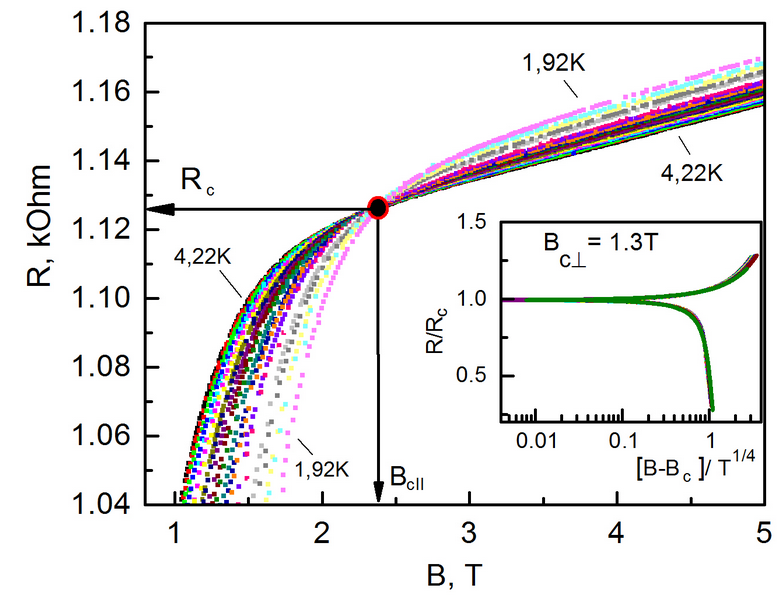
Two-layer heterostructures with island-like conductive interface exhibit the magnetic field induced superconductor-insulator transition: fan-like set of R (T ) curves at different magnetic fields; crossing of R (B ) curves at different temperatures.