Quantum interference structures for probing energy gap and time relaxation of superconducting state
Basic thesises of the method
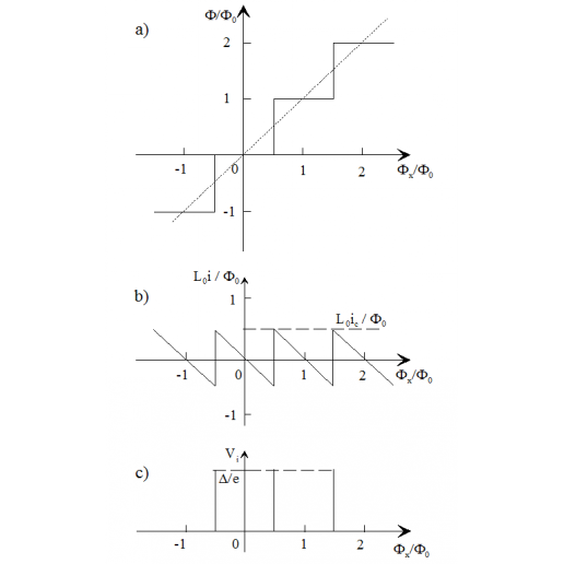
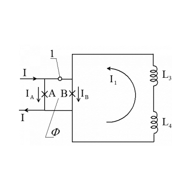
We proposed and investigate now novel method which allows one to make simultaneous measurements of the gap and relaxation time. The method unites two base conceptions. The first of them is Silver and Zimmerman's theoretical prediction saying that the pulsed voltage Vi on superconducting quantum interferometer (SQI) during discrete switching of the circulating current i in it caused by variation of magnetic flux Фx is proportional to the energy gap of the superconductor (Fig.1). Second of them is our proposition of extending the pulse duration to a well-measurable value by shunting the interferometer with a superconducting coil with large inductance L ≈ L3 + L4 which considerably exceeds the inductance L0 of the interferometer (Fig.2).
Fig.1 Estimated dependences of reduced inner magnetic flux Ф/Ф0 (a), reduced circulating current L0i /Ф0 (b) and pulsed voltage Vi (c) on reduced external magnetic flux Фх /Ф0 applied to interferometer with inductance L0. The dependences are received by Silver and Zimmerman in the linear approach under a condition iс ≈ Ф0 /(2L0), Ф0 is a quantum of a magnetic flux.
Fig.2 The electric scheme of a modelling contour of a measuring device in which clamping point contact (CPC) is presented in the form of asymmetric SQI (1) with two micro contacts A and B, having different critical currents and included in branches with different inductances, Ф is the magnetic flux through the SQI contour.
Measurements
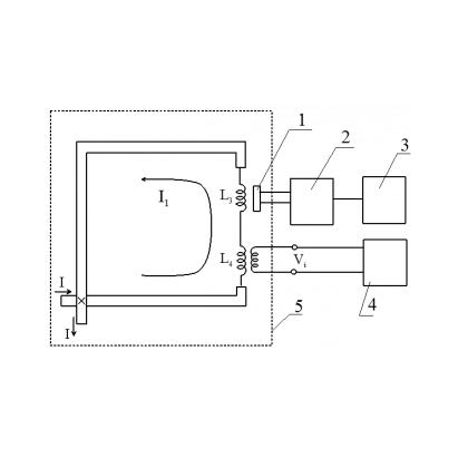
The scheme of the experimental device for measurement of the gap and relaxation time is presented in Fig.3.
Fig.3 The measuring scheme for studying current states of the contour with CPC in a crossing point (x) of niobium microwires: I is a transport current, 1 is the fluxgate detector for measurement of magnetic field of the current I1 flowing through L3 and L4, 2 is the amplifier of the detector signal, 3 is the registrator of the measured magnetic field, 4 is the oscilloscope to display and measure the voltage pulses on Vi the secondary winding of the transformer caused by discrete change of current I1 through the primary winding with inductance L4, 5 is the cryostat.
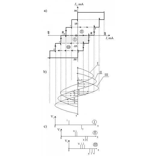
Clamping point contact (CPC) niobium - niobium was used as the interferometer. It was established earlier by Zimmerman with colleagues that the CPC microstructure represents a quantum interferometer with several parallel connected micro contacts. Particularly, a CPC with two micro contacts is possible to make. Such structure is a direct current superconducting interferometer and can be a sensitive element known as dc SQUID. The CPC is prepared by mechanical compression of two crossed niobium micro wires with 70 microns in diameter. Niobium wires form a closed superconducting contour with inductance of about 10-6 H incorporating the above described superconducting interferometer. The other part of the contour consists of two coils (L3 and L4) to couple with a magnetometer fluxgate detector (FG) and to form the primary winding of the pulse transformer. The FG serves for current measurement in the contour. The transformer serves for registration of the voltage pulse arising at the moment of a discrete quantum transition in the interferometer. Initially, the direct current I flows through the CPC while the current in the branch of the contour with inductance 10-6H is practically equal to zero. The interferometer passes in the resistive state with resistance R in short time τ ≈ L0/R as its critical current is achieved. The voltage pulse Vi arises on the interferometer and the contour, while a part of the transport current is switched into high-inductive part of the contour forming the current I1 during the time δt ≈ L/R. Then the interferometer comes back in the superconducting state. A new discrete transition can occur in the interferometer after further increasing of the transport current I that creates magnetic flux equal to Ф0 in the interferometer. As a result, we have a dependence of the current in the contour I1 on the transport current I shown in Fig.4а. Periodic steps of the current in the I1(I) plot correspond to quantum current (i) transitions of the interferometer shunted by superconducting inductance.
Fig.4 The sketch of voltage pulses V*i4 observed on the oscilloscope screen when alternating transport current is driven through the contour: a) initial experimental dependence I1(I) at Т = 4.2K; b) variation of the alternating current during one period at its three various amplitudes I, II, III; c) picture of voltage pulses on the oscilloscope screen (1-8 are numbers of steps of current I1 appeared at various amplitudes of the alternating current).
Results
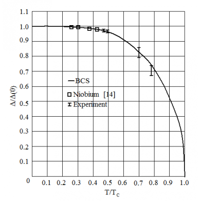
Sweeping this dependence by a low-frequency transport current (Fig.4b) allows us to observe, on the oscilloscope screen (Fig.4c), voltage pulses whose amplitude correspond to the niobium energy gap which turns out to be 2.3 mV at 4.2 К. Experimental values of the gap and calculated curve of temperature dependence of the gap are shown in Fig.5.
The duration of a quantum transition in the interferometer, i.e. the time of relaxation of superconducting state in niobium, can be estimated from ratio of inductance of the interferometer (L0 = 10-13 H) to that of the contour (L = 10-6 H):
τ ≈ (L0 / L) δt . (1)
Thus, as it follows from (1) at δt ≈ 10-5 s, τNb(4.2 K) ≈ 10-12 s. This value is close to Silver and Zimmerman's estimations [1].
Fig.5 Temperature dependence of reduced energy gap of niobium calculated according to BCS theory and the experimental values of the gap obtained from measurements of characteristics of tunnel contacts [2] (open small squares) and from our measurements of voltage pulses Vi on the contour.


